Virtex 5 Block Diagram
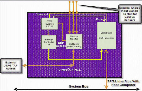
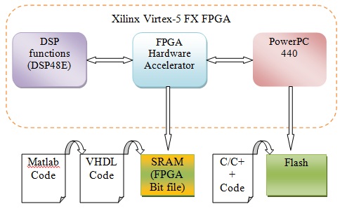
Designing Fpga Based Reliable Systems Using Virtex 5 System Monitor
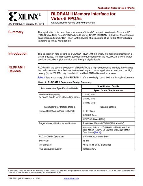
Xilinx Xapp852 Rldram Ii Memory Interface For Virtex 5 Fpgas
Ppt Fig 2 Carry Chain Delay Line A Logic Block Diagram B
Xcm 017
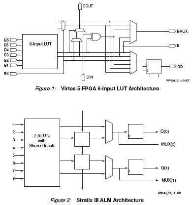
White Paper Advantages Of The Virtex 5 Fpga 6 Input Lut
Https Www Renesas Com Doc Guide An1707 Pdf

Figure 4 2 From Implementation Of Ethernet Aurora And Their
Face Recognition Advinno
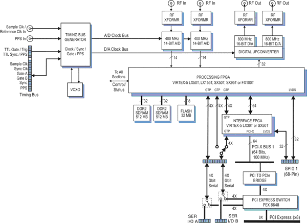
Pentek Model 7856
Https Www Xilinx Com Support Documentation Boards And Kits Ug226 Pdf

15 Virtex 5 Clb Block Diagram 18 Download Scientific Diagram

Configurable Logic Block An Overview Sciencedirect Topics
