Pentium 2 Block Diagram
Pentium Intel 80586
Studopediya Enumerate Elements Of Cache Design
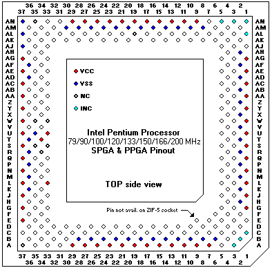
Processor Socket Type
Simplified block diagram of processor tap logic.
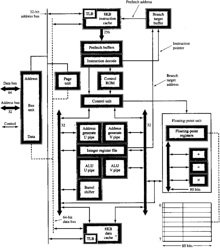
Pentium 2 block diagram. Dandamudi fundamentals of computer organization and design springer 2003. Pentium 4 is a brand by intel for an entire series of single core cpus for desktops laptops and entry level serversthe processors were shipped from november 20 2000 until august 8 2008. 2003 to be used with s. 5th generation intel core.
Indicates the pentium has given control to another local master pentium continues execution from its internal caches cache enable ken if asserted the current cycle is transformed into cache line fill. Pin diagram of pentium. Esp8266 getting started with arduino ide. Tap controller finite state machine.
Intel pentium and celeron processor n3000 block diagram. Externally pentium 4 transfers four data per clock cycle. Microprocessor pin diagram clock clk clock input fundamental timing for the pentium the cpu uses this signal as the internal processor clock. Stp8280 portable tetra radio block diagram 800mhz bands stp8280 circuit description sepura plc.
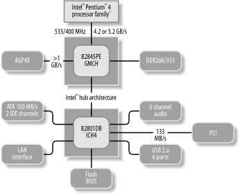
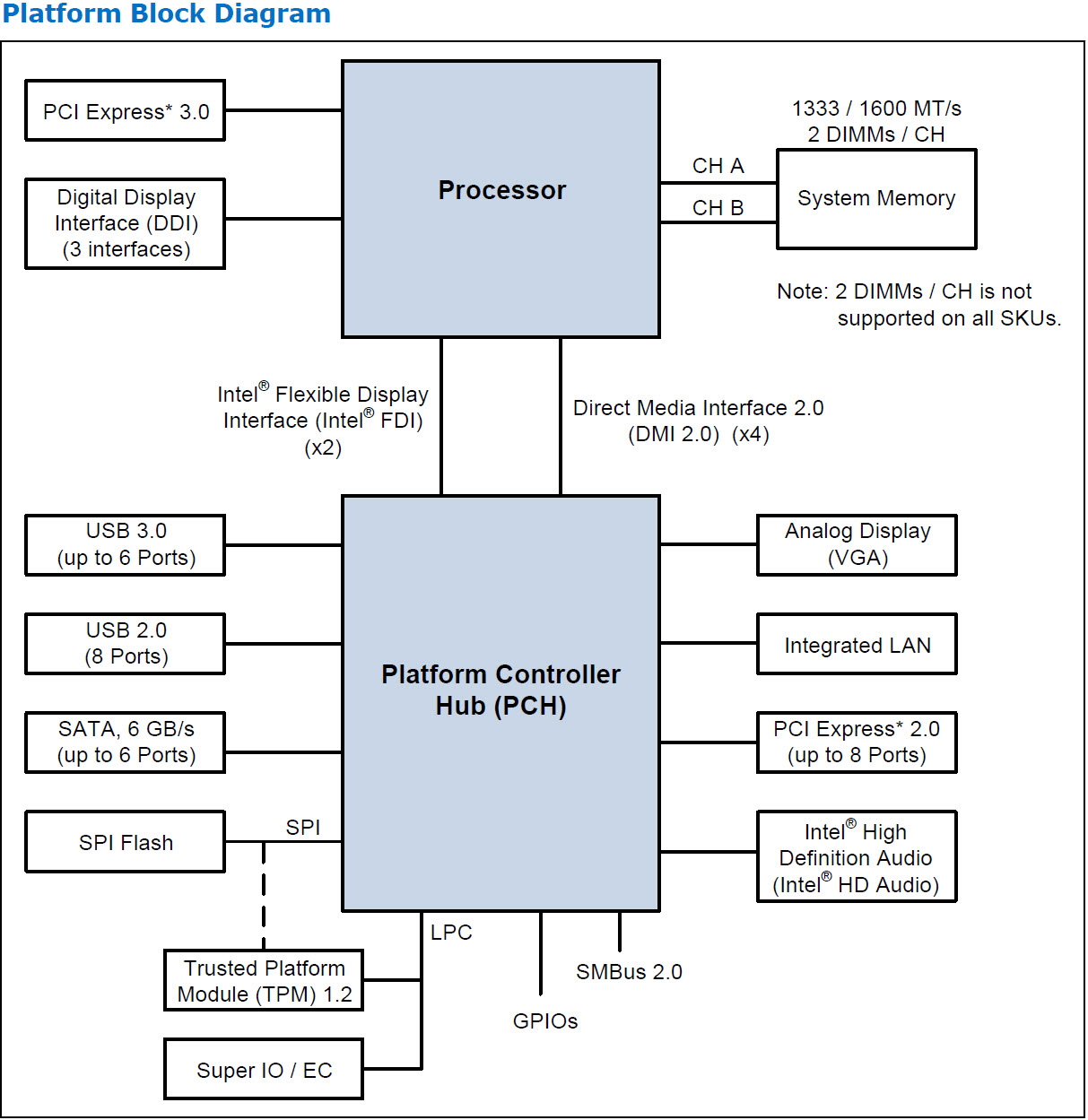
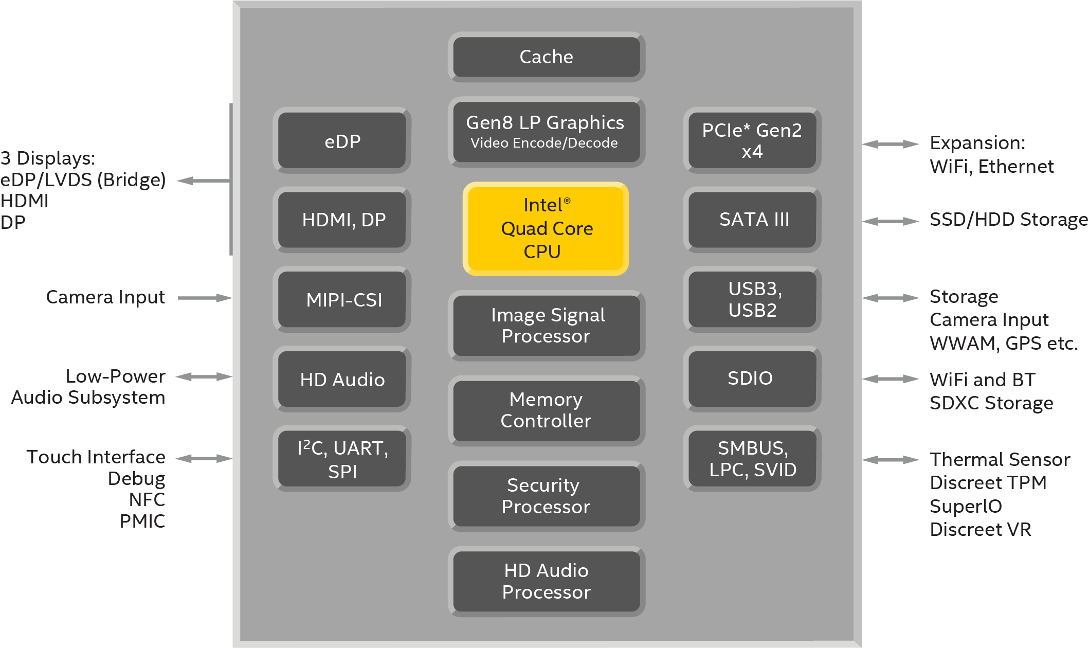
Here are the basic differences between pentium 4 architecture and the architecture from other cpus. Mobile intel pentium processor family and mobile intel celeron processor family june 2015 datasheet volume 1 of 2 order no. For a complete listing of the functions capabilities and connectivity of this platform please review the product documentation. Resultado de imagem para desktop motherboard schematic diagram pdf.
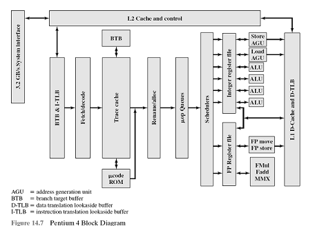
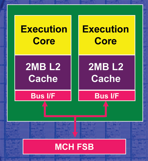
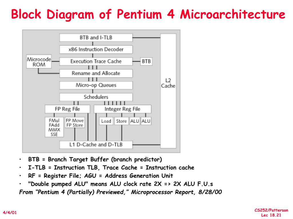
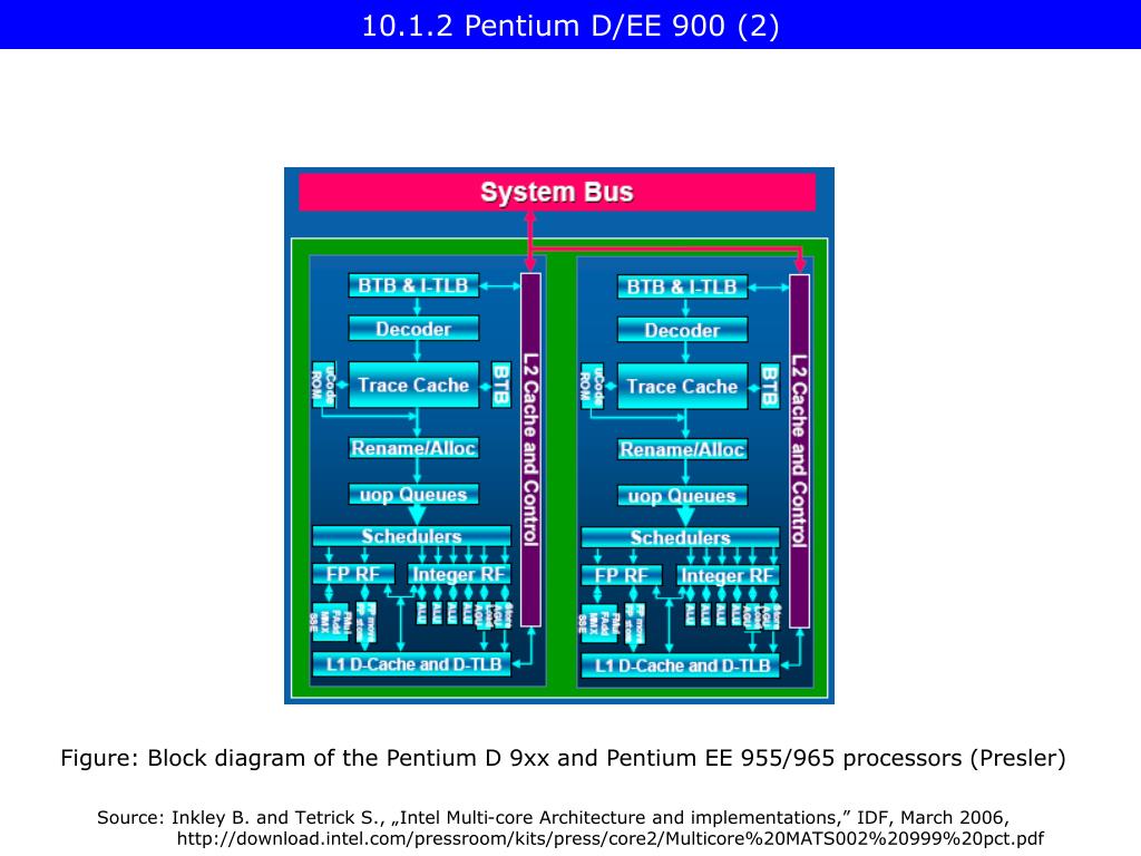
The production of netburst processors was active from 2000 until may 21 2010. This block diagram provides a description of the functions capabilities and connectivity within the platform shown. Pentium 4 processor block diagram fp rf fmul fadd mmx sse fp movefp move fp store 32 gbs system interface l2 cache and control l1 d cache and d tlb store agu load agu schedulers integer rf alu alu alu trace cache renamealloc alu uop queues btb ucode rom btb i decoder 3 3 tlb. When bf is strapped to vss the processor will.
Pentium 2 block diagram pdf. As per msbte syllabus introduction to pentium processor salient features of pentium system architecture superscalar execution. Super heavy lift launch vehicle. Pentium ii processor developers manual 243502 001 october 1997 1997.
Intel 80386 microprocessor chapter 2 notes advance microprocessor. Figures 1 processor platform block diagram.

Mobile Intel Pentium Iii Processor 440mx Chipset Platform Design
A Look At Amd S Dual Core Architecture Amd S Dual Core Opteron
Ppt Cs252 Graduate Computer Architecture Lecture 18 Ilp And
Ppt Dezso Sima Fall 2007 Powerpoint Presentation Free Download
A Novel Way To Massively Improve The Sq Of Computer Audio
Pca 6028g2 00a1e Reference Design Application Processor Arrow Com
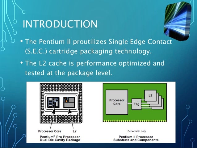
Pentinum 2
Pentium 2 Block Diagram Wiring Diagram
Hyper Threading Wikipedia
