Transistor Wiring Diagram

Npn Transistor Symbol Furthermore Di Box Schematic Furthermore How
Https Encrypted Tbn0 Gstatic Com Images Q Tbn 3aand9gcqcbv 3fkzyegik6o1cey9wrhvc3htua5xq1z1 Tekpppzqyllzdfuar0n61rxefvq Usqp Cau
Https Encrypted Tbn0 Gstatic Com Images Q Tbn 3aand9gcsobl8rfh01anid47dood2i8wyyzke1cphzzj7y9y4ibqyp Zfzcgqwqu4zrzoerqe Usqp Cau
150 ohm 1w.
![]()
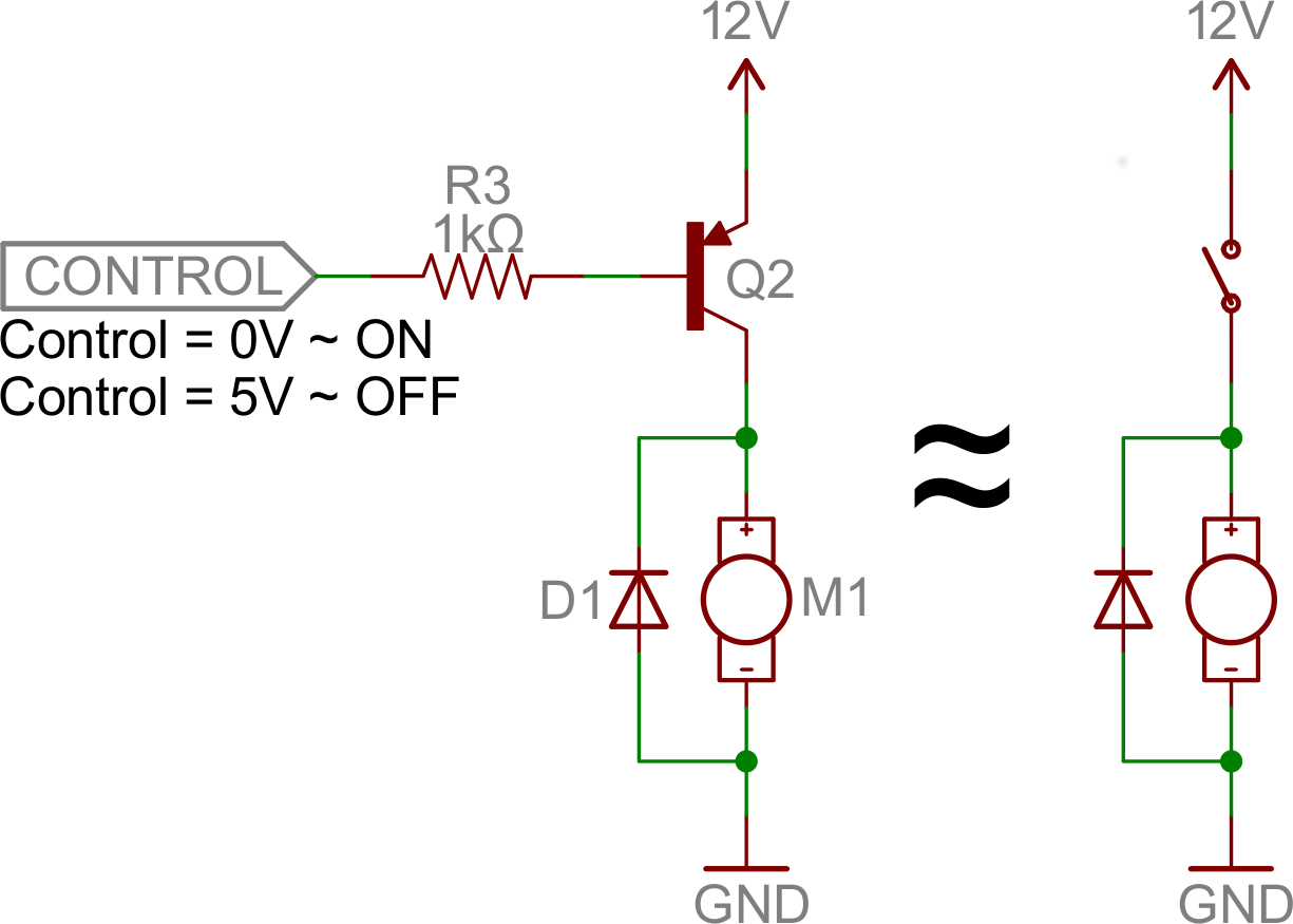
Transistor wiring diagram. The mosfet transistor is an easy way to allow your arduino or other micro controller to handle voltages larger than the 5 volts available for each pin. Mosfet block diagram p channel mosfet. Wiring the mosfet transistor. Connection diagram of pnp and npn transistor outputs for electronic pressure switches 10072011.
For 6v negative ground system change the following resistors. This circuit and wiring diagram. The drain and source are heavily doped p region and the body or substrate is n type. The transistor or drive is the heart of a modern fuel injection system.
The lowermost circuit diagram illustrating the function of the pnp shows the load positioned after the transistor. It is a four terminal device such as gate drain source body. The output of the device that outputs a current will be connected to the base of the transistor. Would anybody be kind enough to advise if this is significant and a function of the type of transistor.
This circuit used for cars with negative ground 12v negative ground system maximum ignition current of 4a and maximum switching speed 500khz. The circuit shown in diagram b is based on an npn transistor. Motorcycles mowers boats etc can also use this circuit. Wiring diagram with the vehicles.
It is also the heart of transmission system and most other systems that have a need for a high speed switching device. This is why the load must be connected differently to the transistor outputs. The uppermost circuit diagram illustrating the function of the npn transistor shows the load positioned before the transistor. One transistor fm receiver by mpf102 by circuit diagram this radio is sensitive enough to tune 20 stations across the fm band some with volume high enough to drive a small pm speaker.
Typical transistor ignition system circuit diagram of 1965 ford and mercury has been viewed 1868 times which last viewed at 2020 06 05 181931 and has been downloaded 1 times which last downloaded at 2014 04 25 1422. 26 out of 100 based on 205 user ratings the typical transistor ignition system circuit diagram of 1965 ford and mercury can be download for free. The p channel mosfet has a p channel region between source and drain. When the switch is pressed a current passes through the resistor into the base of the transistor.
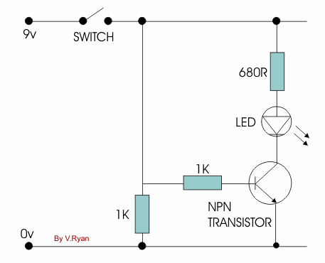
The flow of current is positively charged holes. The setup to set the transistor up as a switch is shown in the diagram below. The transistor then allows current to flow from the 9 volts to the 0vs and the lamp comes on.
Transistors Learn Sparkfun Com

4 Transistor Xor Xnor Circuits Download Scientific Diagram

Https Encrypted Tbn0 Gstatic Com Images Q Tbn 3aand9gcrspcu Zt0nfxyqyv2gq Ouoj6fqagjk77nfyiaes6qb Jvrdoq Usqp Cau

Experiment Transistor Circuit Design
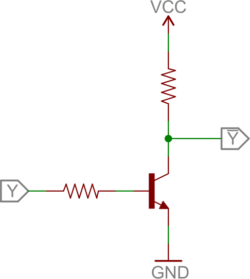
Transistors Learn Sparkfun Com
Https Encrypted Tbn0 Gstatic Com Images Q Tbn 3aand9gcrvscg2zlvenrxjph0fsb5qr1jz3wmvi9czonvurrsfglsx7qvk Usqp Cau

Bipolar Transistor Tutorial The Bjt Transistor

Simple Latch Circuit Diagram With Transistors
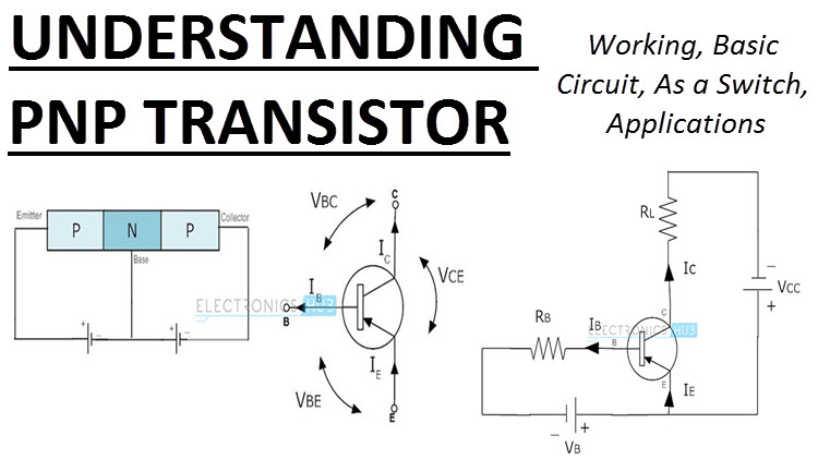
Pnp Transistor Circuit Characteristics Working Applications
